


| Mask Fabrication |
| - Mask Dimensions |
| - Fabrication Process |
| - How to Order |
| Silicon Microfabrication |
| - Capabilities |
| - Facilities |
| One-Stop Services |
Processing Capabilities
Our capabilities include most processes needed to fabricate a microelectromechanical system, from process development to chip fabrication. Single process capabilities, such as photolithography, thin films deposition, wet and dry etching or metrology services are also available.
 Microlithography
Lithography by Mask Aligner/Stepper
E-beam Lithography
Laser Lithography
Thin Film Deposition
PECVD for deposition of SiO2 and SiN thin films
LPCVD for deposition of Si oxide, Si nitride and poly-Si.
RF/DC sputter for depositing thin metal layers
UBM sputter for deposition of oxide and doped TCO films
E-Beam evaporation system for deposition of metals
Thermal evaporation system for deposition of organic layers
 Dry Etching
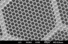
Silicon Deep Etching
Etching of SiO2/Si3N4
Photoresist Stripping
Surface Treatment of Si/Glass
Etching of III-V based compound materials
Wet Etching
Bulk Silicon Micromachining
Etching of SiO2
Etching of Metals
Liftoff of Metals
Metrology/Characterization
Surface profiling
Elipsometer
Back-end processing
Dicing of Si, Quartz, Glass, III-V material
Wire bonding
Trimming of substrates, drilling of holes, surface treatment of polymeric materials
MATERIALS
- Semiconductor Si wafers and Solar wafers
- Silicon on insulator (SOI) wafers
- Mask blanks (soda lime and quartz)
- Glass wafers (Pyrex 7740, quartz, soda lime, etc)
- AIIIBV compounds (GaAs, GaP, InP, InAs, etc)
- Sapphire wafers
- Sputtering targets
- Thin films-Oxide, nitride
- Packing boxes for crystal, wafers, filter, chip, etc
- Optical component
SERVICES
- Fabrication of soda lime/quartz photolithographic masks
- Silicon microfabrication (wet etching, dry etching and wafer bonding)
- Consultancy of fabrication process
- Characterization of microdevices/microsystems
- Consultancy of microfluidics and biological microdevices

Service Hotline:
Tel.: +65-6515 8750
Fax : +65-6515 8795
Email: sales@bondatek.com