


| Mask Fabrication |
| - Mask Dimensions |
| - Fabrication Process |
| - How to Order |
| Silicon Microfabrication |
| - Capabilities |
| - Facilities |
| One-Stop Services |
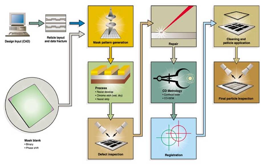
Fabrication Process
Originally the pattern information is created in a drawing package and stored in a database, reformatted and transferred to a lithography tool � laser writer (ALTA3900) or e-beam writer (MEBES5500/5000) in our case � then printed in a layer of photoresist coated onto the photomask blanks.
The imaged pattern is next developed to form a template over the opaque chrome and then the chrome is etched away where the resist is clear. After the etch process is complete, the remaining photoresist is removed, the plate cleaned, and then stored for later use in an optical printer.
MATERIALS
- Semiconductor Si wafers and Solar wafers
- Silicon on insulator (SOI) wafers
- Mask blanks (soda lime and quartz)
- Glass wafers (Pyrex 7740, quartz, soda lime, etc)
- AIIIBV compounds (GaAs, GaP, InP, InAs, etc)
- Sapphire wafers
- Sputtering targets
- Thin films-Oxide, nitride
- Packing boxes for crystal, wafers, filter, chip, etc
- Optical component
SERVICES
- Fabrication of soda lime/quartz photolithographic masks
- Silicon microfabrication (wet etching, dry etching and wafer bonding)
- Consultancy of fabrication process
- Characterization of microdevices/microsystems
- Consultancy of microfluidics and biological microdevices

Service Hotline:
Tel.: +65-6515 8750
Fax : +65-6515 8795
Email: sales@bondatek.com